�о��������òġ�MEMSר��GCM 3060
�������ڣ�2024/11/4 23:25:18
���������
��������
�ղ�����
��ע����
����һ���� ���ٱ��� ���ղء� ����ע��
�о��������òġ�MEMSר��GCM 3060
Gersteltec SU-8 series
������о̩�ƹ������˾
��Ʒ���������� :13��23��66554 �ۿۣ�35��9123��
������о̩�ƹ������˾��������2014�꣬��һ�ҷ�������������IJ�Ʒó�����������ṩ�̡������Ѿ���Ϊ���������Ƴ��������ش�ѧ�о��������ĺ�����飻��˾�������ҳ�̬�ȶԴ��¾ɿͻ����Կͻ�����Ϊ�����ṩ���ʸ�Ч�ʵ�רҵ�����ṩ��Ʒ����������֧Ԯ�������������Ŀ���dz�Ϊһ���²���Ӧ�ü����ƹ�����רҵ��Ӧ�̡�
��Ҫ��Ʒ��Χ ��
һ�� ��̣����Թ�̽����Թ�̽�
���� ��������������Ϳ�㡢��Բ�и�����ͼ��Ͻ�
���� ����������ѧƷ����ӰҺ����ϴ����ȥ��Һ�Ͱ���Һ
Gersteltec SU-8 series
GCM 3060(Conductive SU8-negative tone photo-epoxy
For thin layers)
General information
SU-8 is an epoxy based, chemically
amplified
resist
system
with
excellent sensitivity high
aspect ratios. The primary
applications are Micro-fabricated
mechanical structures (MEMS)
other Microsystems needed non
conductive properties.
Adding metallic particles in the
SU-8 photoresist results in an
enhancement of its electrical
conductivity. GCM 3060 offers an
electrical conductivity of about
101-3 S.cm-2
Datasheet parts��
1 ��Schematics of the process
2 ��Process description
3 ��Processing GCM3060 �C Overview
4 ��Troubleshooting
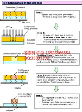
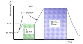
1 / Schematics of the process
2 / Process description
A typical process consists of
-
Substrate preparation
- Spin-coating
- Relaxation time to improve the surface uniformity
- Soft Bake
- Exposure to initiate the cross-linking
- Post Exposure bake (PEB), to cross link exposed regions.
- Development
- Rinse & dry
- Hard Bake (or curing-optional)
- Imaged material (optional: in case of moulding)
- Remove (optional: in case of moulding)
(in chronological order)
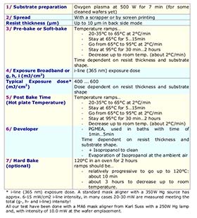
Put the substrate on a furnace / oven at a minimum of 130 ��C for 20 minutes
to remove adsorbed water the substrates surface.
Alternatively use oxygen plasma for 7min at 500 Watts in a Microwave plasma
reactor. This should increase the temperature inside the plasma chamber above
80��C after the 2 firsts minutes.
Spread the resist after cooling down the substrates, with a scrapper or by using
screen printing method.
Softbake the coated substrate in two steps. All the temperature ramps should
be about 2��C/min. Firstly increase the temperature room temperature up
to 65��C. Then let the substrates at 65��C 5 to 15min (depend on the resist
thickness). You can then increase up to 95��C you should let your wafers
as much time as necessary that, when holding them with some tweezers there
are not printed on the SU8 layer! Then you can switch off the power or decrease
temperature until they reach the room temperature.
Expose the coated substrate with the mask in front side mode for very thin
films (less than 5 ��m). Back side mode is preferentially recommended with the
use of an integrated mask between the substrate the conductive
photoresist.
The exposure dose ranges between 400 600 mJ.cm-2, depending on the
structure geometry thickness. More the dose is, more the lateral resolution
will be affected.
Note: Exposure doses refer to i-line (365nm). A stard mask aligner with a
250W Hg light source has approx. 6-15 mW/cm2 i-line intensity, while in
many cases 20-30 mW/cm2 are measured meeting the total (g-, h- i-line)
intensity!
Ideally
you should try some multiple exposure around the given exposure dose
given in Exposure curve. In fact your results may not be exactly the same
because of the UV lamp parameters. So they have to optimise this exposure
dose parameter, simply because your mask aligner is probably not the same.
Post Exposure Bake (PEB): after the delay bake the coated substrate at the
same temperature profile than for the Soft Bake. (Because this step is very
temperature critical furnace baking is not recommended).
This step accelerates the cross-linking of the exposed areas making them
insoluble in the developer.
Develop in PGMEA. When the structure is through-developed (cleared), add
another 10% of the time in a cleaned bath of the total development time to
finalize the side wall profile.
Rinse with Isopropanol. Once there is not any more white traces the
development is then finished. Unfortunately, if you add even more than a
minute, you would increase the composite layer that should unstuck the
substrate.
Dry the wafers just letting them at the ambient air, on a wet bench with an
appropriate air flow (exhaust).
Hard-bake: use the same temperature profile than for the Soft Bake, with a
final temperature of 120 ��C. The electrical conductivity will be enhanced by one
decade.
3 / Processing GCM3060 - Overview
4 / Troubleshooting
White traces after development: This is only because there is still some unexposed
SU8 not totally developed. In fact unexposed SU8+Isopropanol makes a white complex
that you can find on your wafers.
In the other side, just pay attention to not develop to much time. Otherwise you could
unstuck the composite layer the substrate.
