深圳市芯泰科光电有限公司,创立于2014年,是一家服务于微电子领域的产品贸易及技术服务提供商。我们已经成为国内微电子制程领域和相关大学研究所信赖的合作伙伴;公司秉持以忠诚态度对待新旧客户,以客户满意为导向,提供优质高效率的专业服务,提供产品行销及技术支援解决方案。我们目标是成为一家新材料应用技术推广服务的专业供应商。
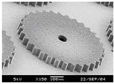
GM 1040 is an epoxy based, chemically amplified resist system with excellent sensitivity high aspect ratios. The primary applications are Micro-fabricated Mechanical Structures (MEMS) other Microsystems. Examples are sensors, micro-fluidic components, electronic coils, inkjet print head nozzles, multi-chip modules, actuators, LCD spacers moulds for plastic, stamps for hot embossing electroplating.
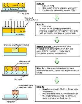
1/Schematicsoftheprocess
2 /Process description
A typical GM 1040 process consists of
- Substrate preparation (dehydration, cleaning…)
- Spin-coating
- Relaxation time to improve the surface uniformity
- Soft Bake Exposure to initiate the cross-linking
- Post Exposure bake (PEB), to cross-link exposed regions.
- Development Rinse & dry
- Hard Bake (or curing-optional)
- Imaged material (optional: in case of moulding)
- Remove (optional: in case of moulding)
(in chronological order)
? Put the substrate in an oven at a minimum temperature of 130 °C during at least 20 minutes to remove adsorbed water the substrate surface. Alternatively use an oxygen plasma for 7 min at 500 Watts in a Microwave plasma reactor. This should increase the temperature inside the plasma chamber above 80°C after the 2 first minutes. Stard HMDS procedure is not recommended for GM 10series on SiO2 based wafers.
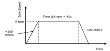
? Spin-coat the resist after cooling down the substrates, at the wanted speed level during 40 seconds. The acceleration deceleration ramps should be about 100 rpm/s to avoid any contamination of the chuck the pins by the GM 1040. Otherwise, some resist on the vacuum system should damage your spin coat system.
? Relax (optional) the resist 5 min up to 15 min, depending on the resist thickness. If there are some bubbles just after spin-coating they can be burst using a clean thin tip. The created hole should be removed during the required time. Finally this relaxation time should improve the uniformity of the layer, evaporate some portion of solvent.
? Softbake the coated substrate in two steps. All the temperature ramps should be about 2°C/min. Firstly increase the temperature room temperature up to 65°C. Note that for you can even start 50°C. Then let the substrates at 65°C 5 to 10min (depending on the resist thickness). The temperature can be then increased up to 95°C the wafers should be let as much time as necessary that, when holding them with some tweezers there are not printed on the GM 1040 layer! Then you can switch off the power or decrease temperature until they reach the room temperature.
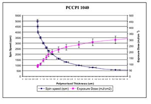
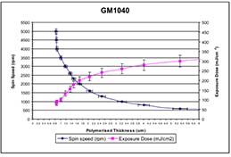
? Expose the coated substrate with the mask. This exposure dose adjusts the negative wall profile whom slope is closed to 90°. Have a look on the exposure curve to choose as a function of your thickness the dose that give not any cracks, un-sticking or “stairs effect”.
Note: Exposure doses refer to i-line (365nm). A stard mask aligner with a 350W Hg light source has approx. 6-15 mW/cm2i-line intensity, while in many cases 20-30 mW/cm2 are measured meeting the total (g-, h- i-line) intensity!
Ideally you should try some multiple exposure around the given exposure dose on the Exposure curve. In fact your results may not be exactly the same because of the UV lamp parameters. So you have to optimise this exposure dose parameter simply because your mask aligner is probably not the same than our.
? Delay time: Keep the coated substrate at room temperature after the exposure for at least 10 minutes. In this delay time some chemical species will diffuse on the exposed parts giving more homogeneity on the amplification phenomenon.
? Post Exposure Bake (PEB): after the delay bake the coated substrate at the same temperature profile than for the Soft Bake. (Because this step is very temperature critical, oven baking is not recommended). This step accelerates the cross-linking of the exposed areas making them insoluble in the developer.
? Develop in DRGM. When the structure is through-developed (cleared), add another 10% of the time in a cleaned bath of the total development time to finalize the side wall profile.
Rinse with Isopropanol. Once there is not any more white traces the development is then finished. Unfortunately, if you add even more than a few seconds, the GM 1040 layer that should be unsticking the substrate.
Dry the wafers just letting them at the ambient air, on a wet bench with an appropriate air flow (exhaust).
? Hard-bake (optional) the coated substrate if after drying there are some unstuck GM 1040 or cracks. Only the smallest cracks (<5 μm) will be totally removed after this step
Optional…
? Imaged material (optional: in case of moulding): deposition of you material by sputtering, electrodepositing…
? RemoveGM1040: using the Gersteltec GM 1040 striper
4/ProcessingGM1040-Overview
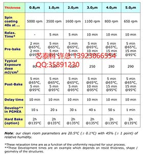
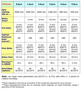
5/Typicalprocesses(0.8μm,1,2,3,45μm)
Firstly,thewaferpreparationshouldbeasmentionedpreviously(Oxygenplasmaat 500Wformin7min(forsomecleanedwafersyet)…).
6 /Troubleshooting
? Cracks: theses drawbacks appear as a function of the exposure dose, temperature ramps taken Pre-bake time. Try to increase the exposure dose range by some x10 mJ/cm2, if you want to try multiple exposure. Consequently, you will see the quality of the surface changing.
? White traces after development: This is only because there is still some unexposed GM 1040 not totally developed. In fact unexposed GM 1040+Isopropanol makes a white complex that you can find on your wafers. In the other side, just pay attention to not develop to much time. Otherwise you could unstuck the GM 1040 layer the substrate.
Appendix
Our machines…:
-Spin-coating : RC-8 Karl Suss
- Mask aligner : MA6 mask aligner Karl Suss with a 250W Hg lamp , with intensity of 10.0 mW at the wafer emplacement.
-Hotplates Karl Suss.
- Thickness measurements : AlphaStep 500.
